Committing the future of advanced manufacturing
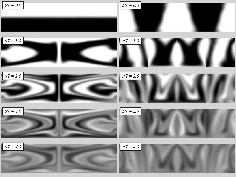
Chaotic cavity flow
(Source : Ho Jun Kim and Ali Beskok 2007 J. Micromech. Microeng. 17 2197)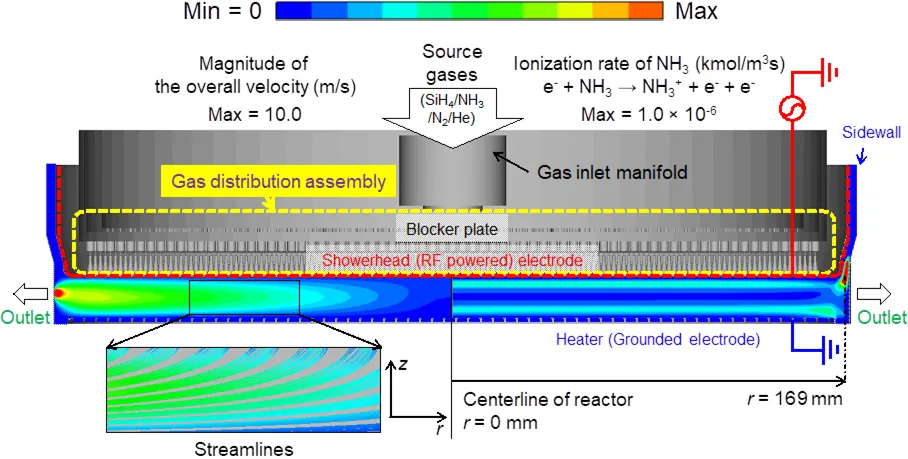
Capacitively Coupled Plasma Reactor
(Source: Journal of Applied Physics 118, 043304 (2015))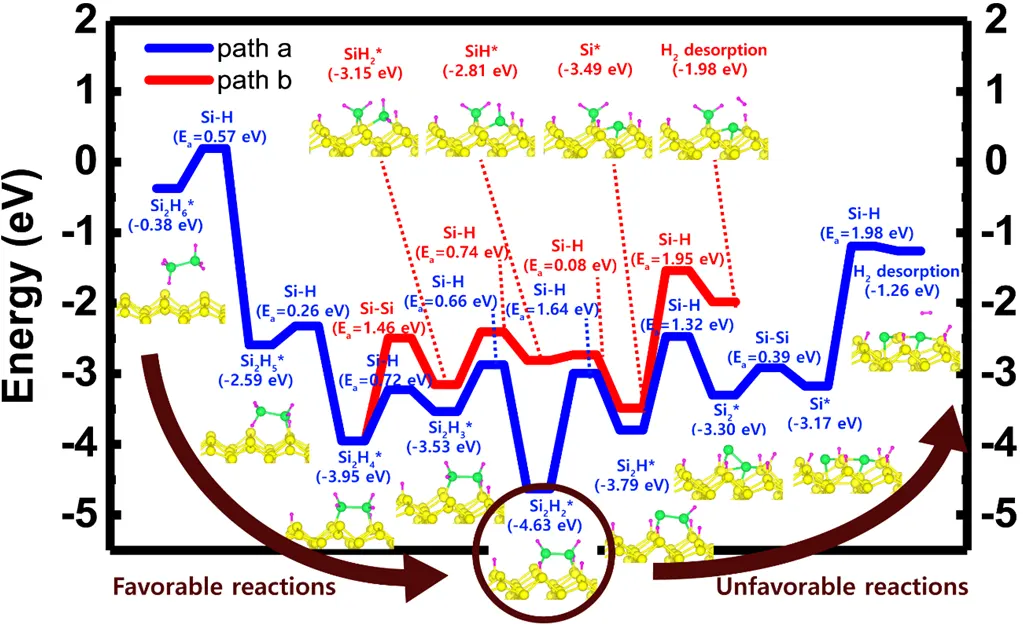
Molecule dissociation and deposition of Si2H6
(Source: Applied Surface Science Volume 496, 1 December 2019, 143728)


Chaotic Systems and Plasma Physics Laboratory is a research group within the Department of Mechanical Engineering specializing in advanced computational fluid dynamics (CFD), molecular dynamics (MD), and plasma simulations for semiconductor and display processing equipment. Our lab employs a wide range of state-of-the-art modeling techniques—including 2D/3D numerical simulations, Particle-in-Cell/Monte Carlo Collision (PIC-MCC) methods, Molecular Dynamics (classical MD and Reactive MD), and Density Functional Theory (DFT)—to precisely analyze the complex fluid dynamics and chemical reactions occurring in plasma processing environments. Through these approaches, we systematically investigate microscale phenomena such as plasma distribution, transport of reactive species, thin-film deposition mechanisms, surface reactions, and etching behavior inside plasma reactors.
We place a strong emphasis on optimizing key materials and structural components within processing equipment—such as wafers, electrodes, and chamber sidewalls—to meet the demands for high precision and high efficiency in semiconductor and display manufacturing. By quantitatively evaluating how material properties (e.g., dielectric constant, thermal conductivity) and geometric configurations influence plasma characteristics and film-thickness uniformity, we develop practical design guidelines that can be readily applied in industrial settings. Simulation results are rigorously validated through comparison with experimental data to ensure accuracy and reliability.
Recently, the laboratory has expanded its research into data-driven approaches by integrating machine learning with physics-based simulations. Using large-scale datasets generated from DFT calculations, we develop machine-learning models capable of rapidly predicting the activity and stability of catalysts for key energy-conversion reactions such as the hydrogen evolution reaction (HER) and oxygen evolution reaction (OER). This combined computational–data-driven framework accelerates the discovery and optimization of novel materials, contributing both to clean-energy technologies and next-generation semiconductor processes.
The Chaotic Systems and Plasma Physics Laboratory actively collaborates with government agencies—including the Ministry of Trade, Industry and Energy and the Ministry of Science and ICT—as well as national research institutes and industrial partners. Through these collaborations, we address real-world engineering challenges and drive technological innovation. Our researchers routinely present their findings at major domestic and international conferences, maintaining a leading role in advancing the field.
Ultimately, the Chaotic Systems and Plasma Physics Laboratory aims to pioneer the future of semiconductor and display industries by combining cutting-edge CFD, plasma simulation, molecular dynamics, and data-driven materials design. By integrating experiments, simulations, and data science, we are committed to developing high-value processing technologies and breakthrough materials that will shape the next era of advanced manufacturing.
In our Lab, We focus on industry-sponsored research related to new equipment development.
| Rank 2016 |
Rank 2018 |
Company | Share(%) 2018 |
|---|---|---|---|
| 1 | 1 | Applied Materials | 20.9 |
| 2 | 2 | Lam Research | 15.9 |
| 4 | 3 | Tokyo Electron | 14.1 |
Source : Gartner (April, 2019)
Importance of understanding plasma behavior
Experimental limitations
Costly, time-consuming recipe experiments
Quantitative analysis recipe experiments
Process optimization through condition analysis
Growing demand for Multiscale
Accuracy limits of single-scale analysis
Growing need for plasma-wafer coupled analysis
Expanded use of simulations for recipe optimization

Key Technology
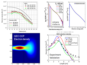
Experimental data: Korea Institute of Fusion Energy
Plasma distribution under parameters
Reactor design improvements
Providing process results
Key Technologies
Project demand